Following is additional information on using Kaamos W-DAC board. Please also see the product description. If something is still unclear, please contact us. We will try to update the information based on feedback.
Power supply
The ADC board requires 5V for digital (VD), 6V for analog references (VA), and +/-15V (VP/VN) for output stage. 5V should be 5V (max 5.5V) but +/-15V can be lower, for example +/-12V works fine. If you don’t have 6V references supply, you can solder 2x ferrites or 0R resistors to take the reference supply from +15V. You can also just connect VP (+15V) to VA (6V) outside the board; however be careful if using other Kaamos boards in the system as VP-VA connection may not be allowed in all boards.
See current consumption per supply on product page.
If you use a Kaamos power supply, all four supplies are provided in one 6-pin Molex Micro-Fit connector. If not, you can solder your own power supply wires in the Molex footprint or order a power cable, cut one end and connect it in your power supply.
Note that the input stage consumes good amount of power and the board gets fairly hot under the opamps.
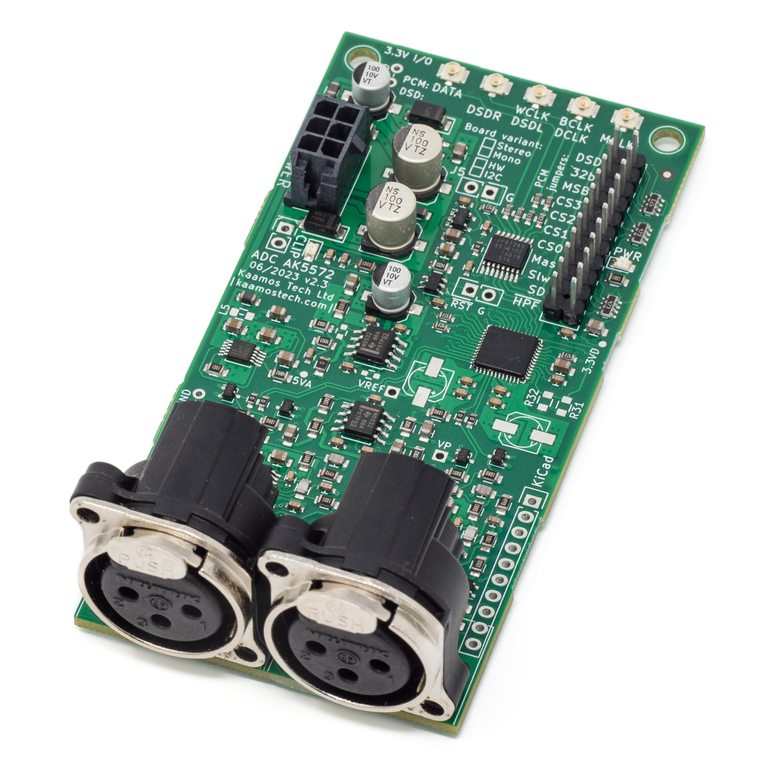
I2S signals
ADC AK5572 has I2S digital serial interface consisting of following four signals:
- MCLK – Master Clock
- BCLK – Bit Clock
- WCLK – Word Clock (sometimes also referred as LRCK)
- DATA
MCLK is always input and DATA is always output. BCLK and WCLK direction depends on Master/Slave setting. MCLK must be in sync with BCLK and WCLK when provided externally.
All these are provided with U.FL connectors. Signal level is 3.3V and there is no termination. For more information on using U.FL cables, please see a dedicated post.
Analog inputs
The board can be ordered with mono or stereo input, and unbalanced RCA or balanced XLR configuration.
Mono version duplicates input circuits and sums inputs, achieving 3dB dynamic range improvement due to uncorrelated noise. THD+N sees slight improvement in most units as well.
Nominally the boards are built for symmetrical XLR inputs and it provides the best performance. For Unbalanced input performance is boosted by using 6dB gain which also brings the input sensitivity to more suitable level for RCA. This gain can be added by bottom-side 0R resistors or jumper links.
Therefore, all input option changes are only small BOM changes.
Control mode
Control mode between HW and I2C are chosen with one bottom-side resistor.
HW control
In HW mode configuration is done with jumper links. In PCM mode the configuration is as follows:
- PCM/DSD
- No jumper link is PCM.
- Master/Slave (PCM only, DSD is always Master)
- No jumper link is Slave.
- Clocking and sample rate selection
- In Slave mode leave all CS links open for automatic clock selection.
- In Master mode refer to AK5572 datasheet how to configure the sample rate.
- Digital filter selection (PCM only)
- Default Sharp filter when no jumper links.
- Choose Slow by closing ‘Slw’ link but leaving ‘SD’ open.
- Choose Short Delay version of Sharp or Slow filter by closing the ‘SD’ link.
- Digital high-pass filter
- Enabled without jumper link. Disabling the HPF causes DC level in the digital signal.
- 32b/24b data
- 24b data without jumper link. This doesn’t have have any practical meaning, performance is the same. It is there because the link may be needed in DSD mode for different function.
If no jumper links are placed, the board works for most PCM Slave use cases without any configuration as clocks are set automatically.
When using DSD, close DSD and Mas links. Clocks are then chosen by DSE0, DSE1, and DCKS links; see bottom side silkscreen of the PCB.
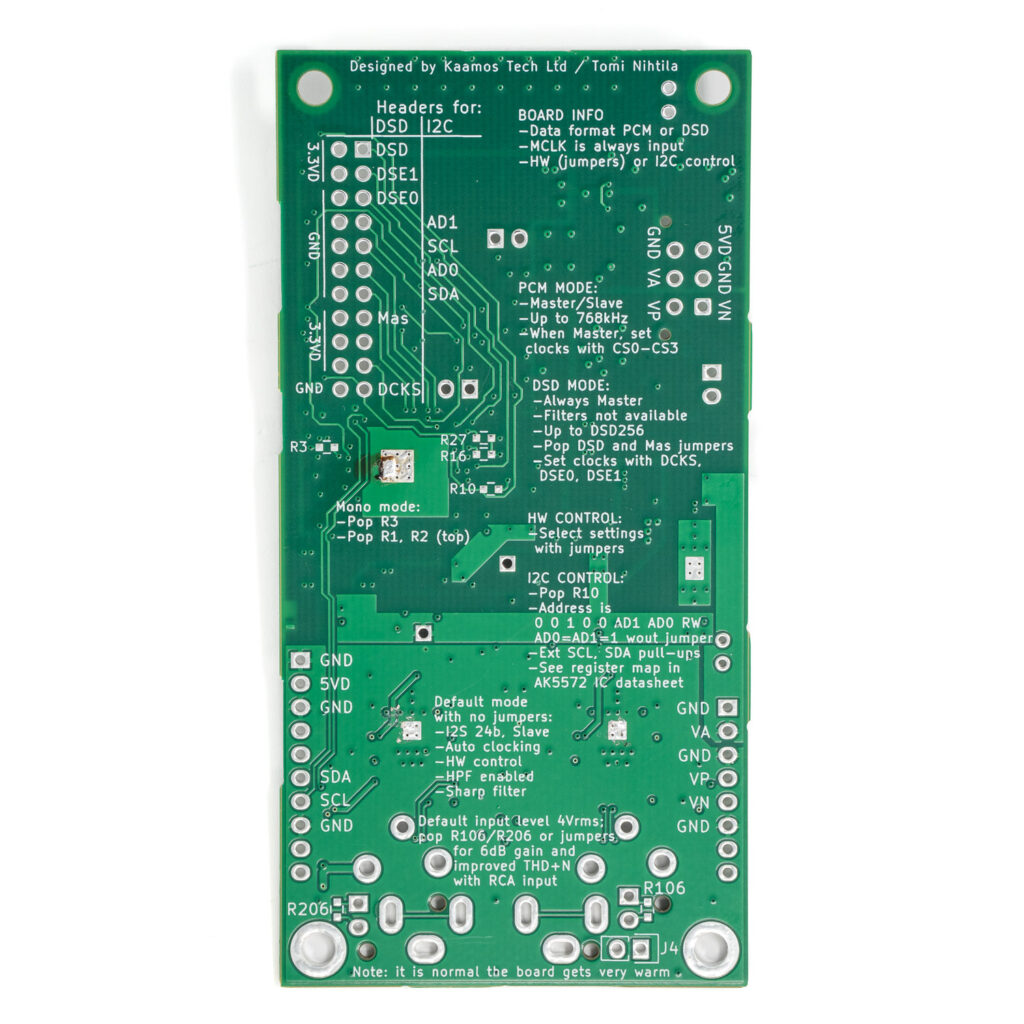
I2C control
In I2C mode configuration is done via register programming. In this case connect SCL (CS2 jumper link) and SDA (CS0 jumper link) and change I2C address if needed (CS1 and CS3). There are weak 47k pull-ups for SCL and SDA so you may want to use stronger ones near the host.
Default address is 0010 0 AD1 AD0 RW where AD1 and AD0 are 1 by default but can be changed with jumper links, and RW is Read/Write bit. For register configuration see AK5572 datasheet. For now we do not have example register writes as the board has practically the same functionality even in HW-control mode.
Input overloading
There is a simple input protection circuit but overloading the input for long period of time may damage the board, or overloading it too much may damage it instantly. Unfortunately we cannot give signal levels or times where the damage occurs. It is not overly sensitive; we have not damaged any boards in our own testing, but a word of warning that any protection will eventually fail if stressed enough. For normal audio use this should not be an issue.
Clipping LED
There is an onboard LED to light when input signal clips. There is also a header/holes next to it where you can wire an external LED to front panel if needed.
More information
See a post on adding S/PDIF outputs to ADC AK5572 and ADC AK5572 product page.