
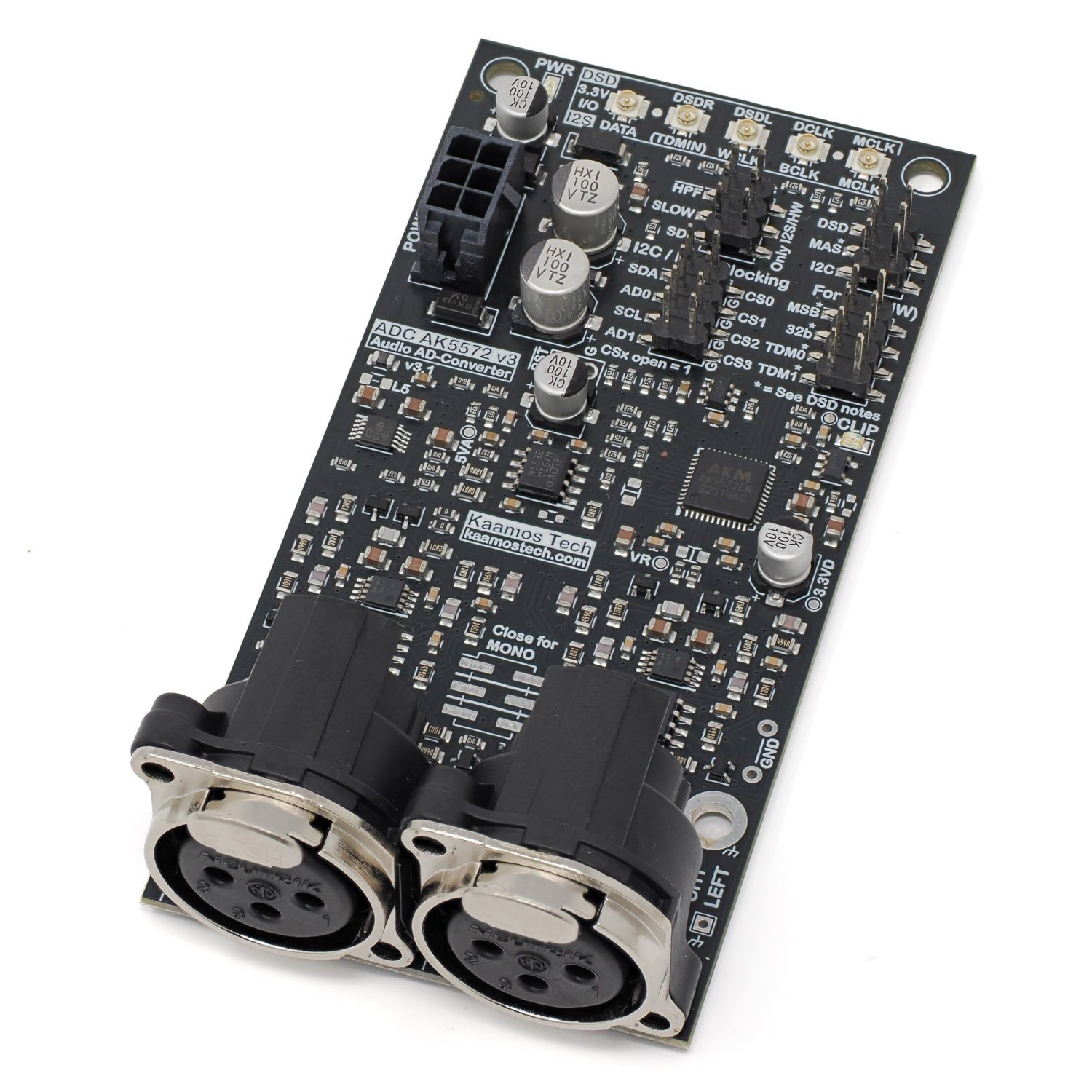
This additional information provides further guidance on using the Kaamos ADC AK5572 v3 board. If anything remains unclear, feel free to contact us.
Power supply
The ADC board needs 5V for digital (VD), 6V for analog references (VA) and +/-15V (VP/VN) for the input stage. The 5V should be 5.0V (maximum 5.5V) but the +/-15V can be lower; for example +/-12V is perfectly acceptable. If you don’t have a 6V supply you can use the reference supply from VP either externally or by soldering L5 onboard. However be cautious if you’re using other Kaamos boards in the system as VP-VA connections might not be permitted on all boards.
The supply inputs only have a simple TVS protection which provides rudimentary over-voltage and polarity ‘protection’ – the latter by shorting the source.
See current consumption per supply on the product page.
A Kaamos power supply (such as One Four All) offers all four supplies in a single 6-pin Molex Micro-Fit connector. Alternatively, you can purchase a power cable, cut off one connector and solder the wires to your own power supply.
Note that the input stage does heat up and the whole board can get very warm under the opamps.
Analog inputs
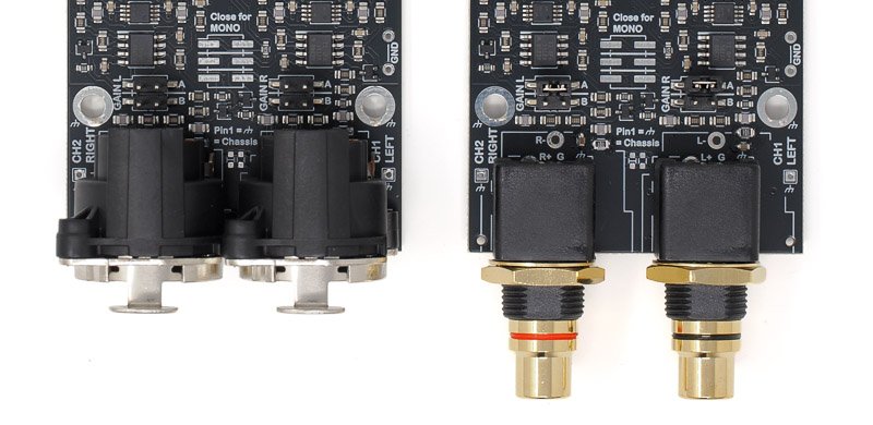
The board is available in two variants catering to different input types: stereo XLR and stereo RCA. The PCB remains the same but features different connectors and a few minor changes to the BOM. It also supports mono operation although we currently don’t offer mono variants.
Gain header offers multiple gain settings with the following maximum input voltage levels:
- 0dB (no jumper link): 4.0 Vrms input (default for XLR).
- 6dB (A closed): 2.0 Vrms input (default for RCA).
- 9,5dB (B closed): 1.3 Vrms input.
- 12dB (A and B closed): 1.0 Vrms input.
Please be aware that input signals between the connectors and input circuits are crossed to align with the connector order in W-DAC, also meaning the connector order is different in ADC AK5572 v2 and v3. Consequently, the gain header next to the left channel sets the gain for the right channel and vice versa. The channel markings are clearly indicated on the silkscreen for both the connectors and the gain headers.
Digital outputs
The board supports multiple digital output formats:
- PCM
- I2S or MSB, both also in TDM-mode.
- Master or Slave.
- Up to 32bit and 768kHz.
- DSD
- Always Master.
- Up to DSD256.
Signal mapping
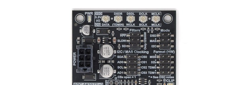
The interface uses five signals in UFL connectors, four of which are typically employed. The table below shows the mapping between the UFLs and signals.
| Format | UFL pins | DATA | DSDR / (TDMIN) | DSDL / WCLK | DCLK / BCLK | MCLK |
|---|---|---|---|---|---|
| PCM: I2S or MSB | DATA output | Not used | WCLK | BCLK | MCLK (input) |
| PCM: TDM-mode | DATA output | DATA input | WCLK | BCLK | MCLK (input) |
| DSD | Not used | DSDR (output) | DSDL (output) | DCLK (output) | MCLK (input) |
Explanation of the signals:
- MCLK – Master clock. Always input.
- BCLK – Bit clock. Input in Slave mode, output in Master mode.
- WCLK – Word clock. Input in Slave mode, output in Master mode.
- DATA – Data output.
- TDMIN – Data input in TDM mode where multiple boards are daisy-chained.
- DCLK – DSD bit clock. Always output (Master mode only).
- DSDL – DSD Left channel bit stream output.
- DSDR – DSD Right channel bit stream output.
All these are provided with U.FL connectors. Signal level is 3.3V and there is no termination.
I/O back-powering
I/O back-powering (or back-drive) can occur if input clocks are active but the ADC isn’t powered on. These clocks partially power the 3.3V rail through the ADC IC’s ESD-protection diodes, possibly causing a failed start-up when the ADC is finally powered up. While system power-sequencing helps prevent this (if it is even an issue), certain types of clock buffers (buffers with Ioff feature) can also mitigate the issue. The ADC AK5572 v2 included these buffers but they were removed in v3 for reasons like supporting TDM and reducing latency in specific applications.
MCLK still has an Ioff buffer to prevent back-powering. Therefore, if the clocks can’t be turned off when the ADC is powered down, a workaround is to run the ADC in Master mode and prevent back-powering. Alternatively, you can reset the ADC IC using the provided (unpopulated) reset header.
Control mode
Control mode between HW and I2C are chosen with ‘I2C’ jumper link (open = HW, closed = I2C).
Note that Master/Slave selection is done with jumper link even in I2C mode (MAS link: open = Slave, closed = Master).

HW control
In HW mode configuration is done with jumper links. First, choose the mode:
- PCM/DSD (‘DSD’ jumper link):
- Open = PCM, closed = DSD.
In PCM mode, the rest of the configuration is as follows:
- Clocking and sample rate selection (‘I2C / MAS Clocking’):
- In Slave mode leave all ‘CS’ links open for automatic clock selection.
- In Master mode refer to the clocking table below or AK5572EN datasheet how to configure the sample rate.
- Digital filter selection (filters work only in PCM mode up to and including 192kHz):
- ‘nHPF’ is digital high-pass filter (open = enabled, closed = disabled). If disabled, the signal has rather high DC-level.
- ‘SLOW’ and ‘SD’ select slow and short delay versions of the filters, respectively. There are four filters:
- Default Sharp filter is selected when both are open.
- Short Delay Sharp filter: ‘SLOW’ = open, ‘SD = closed.
- Slow filter: ‘SLOW’ = closed, ‘SD = open.
- Short Delay Slow filter: ‘SLOW’ = closed, ‘SD = closed.
- Data format ‘FORMAT (HW)’:
- MSB: open = I2S, closed = MSB.
- 32b: open = 24bit data, closed = 32bit data. This doesn’t have any practical meaning since effective number of bits is less than 24.
- TDM1/TDM0: TDM mode, see AK5572 datasheet (Table 9, page 36) for all the options.
For most use cases the defaults are fine and no jumper links need to be placed. The defaults are:
- PCM Slave, automatic clock selection.
- 24b I2S.
- Sharp filter and high-pass filter enabled (filters don’t work at higher than 192kHz rates).
In DSD mode some of the jumper links change functionality:
- First, close ‘DSD’ and ‘MAS’ jumper links.
- ‘FORMAT (HW)’ links are now:
- MSB = DSDSEL0 (open = 1).
- 32b = DSDSEL1 (open = 0).
- TDM0 must be open.
- TDM1 must be open.
- ‘Filters’ / ‘nHPF’ link is now DCKS (open = 1).
- Note that filters are not functional in DSD mode.
I2C control
Enter I2C control mode by closing the ‘I2C’ jumper link.
In I2C mode, configuration is achieved through register programming. The I2C signals SCL and SDA are accessible via the ‘I2C / MAS Clocking’ header. There are weak 47k pull-ups for SCL and SDA so stronger ones are advisable near the host.
The default I2C address is 0010 0 AD1 AD0 RW where AD1 and AD0 are 1 by default but can be set to 0 by closing the jumper links ‘AD1’ and ‘AD0’, respectively. RW is Read/Write bit. Please note that most AKM audio ICs use the same 4-bit address space, and if you use Kaamos W-DAC or DAR 18, for example, they use the same address space.
For register configuration see AK5572EN datasheet. All the configuration options discussed in HW-control are available in the registers – except Master/Slave selection that must be done with the jumper link.
For a quick power-up, the following writes used in the board evaluation bring up the ADC to a state similar to HW-control default configuration:
// ADC I2C-address (7-bit address)
var adc=0x13;

// ADC is active after power-up. Let's set reset state during configuration.
Write(adc, 0x01, 0x00);

wait(0.1) // probably not needed

// Set CKS and DIF bits for Auto clocking in Slave mode. Data format is 24-bit I2S. Digital high-pass filter is on.
Write(adc, 0x02, 0x7B);

// Digital filter is left to default.

wait(0.1) // probably not needed

// Take ADC out of reset state
Write(adc, 0x01, 0x01);
Note that when the ADC is powered on, there is around 1 second power-up delay. Therefore, do not start I2C communication right after power-up.
Clocking
For comprehensive clocking guide and all the options, please refer to AK5572EN datasheet. However, the following gives some guidelines in setting up the ADC.
MCLK
The best MCLK options are 24.576MHz (for 48k family of sample rates) or 22.5792MHz (for 44.1k family of sample rates). They are the most commonly used and all AK5572EN sample rates support them. For other clock rates, see the datasheet how it is supported (Tables 2 to 4 on page 32).
PCM Slave
When the ADC is set to Slave mode and auto-clocking (no ‘CS’ jumper links), it adapts to the incoming clock rate. Note that BCLK and WCLK must be in sync with the MCLK (divided from the MCLK).
PCM Master
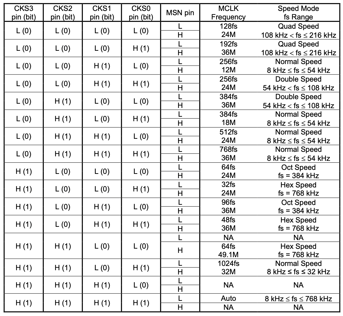
In Master mode user must set CS jumper links (HW) or CKS bits (I2C) to configure the sample rate and clocking. The ADC takes in MCLK and generates BCLK and WCLK from it with internal dividers. The table below is from the AK5572EN datasheet (table 5, page 33) showing the options.
Let’s assume MCLK is 24M (e.g. 24.576MHz; these are all relative so only the ratios matter). If you want 192kHz sample rate, follow the first row (128fx, 24M). Regarding CS0-3 jumper links, closed=0 and open=1. Therefore, the first row means all four links are closed. For 48kHz (512fs, 24M), close CS0 and CS3.
DSD clocking
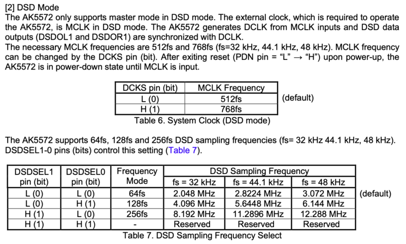
Below is a capture from the datasheet page 34 regarding DSD clocking. The concept of sample rate is a bit different with DSD, but to set it for DSD256 with ’48kHz DSD sampling frequency’, we need:
- DCKS = 0.
- HW mode: close ‘nHPF’ link.
- DSDSEL0 = 0.
- HW mode: close ‘MSB’ link.
- DSDSEL1 = 1.
- HW mode: close ’32b’ link.
Input overloading
There is a simple input protection circuit but overloading the input for a long period of time may damage the board, or overloading it too much may damage it instantly. Unfortunately, we cannot give signal levels or times where the damage occurs. It is not overly sensitive; we have not damaged any boards in our own testing, but a word of warning that any protection will eventually fail if stressed enough. For normal audio use this should not be an issue.
Clipping LED
There is an onboard LED to light when the input signal clips. There is also a test point next to it where you can wire an external LED to front panel if needed.
Note that based on our tests the clipping LED doesn’t work in DSD and TDM modes, although the datasheet doesn’t state so.

Future options
The PCB supports mono operation but currently we don’t offer mono variants. If you need mono units, please contact us. Alternatively, remove one connector and populate the MONO header (or short the contacts).

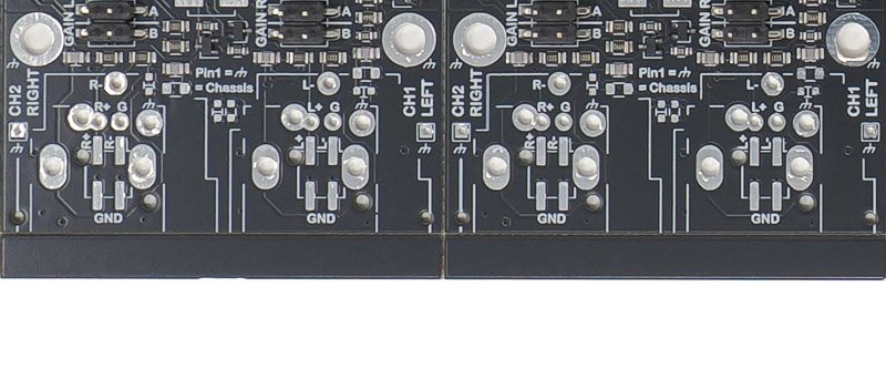
Besides XLR and RCA, the inputs support 2×2 pinheader input (under the XLR/RCA). This allows for designing a stackable add-on board, e.g. for extra input gain or attenuation. If you want to purchase the ADC without connectors and design your own add-on, or want us to design the add-on, please contact us.
Non-audio applications
ADC AK5572 is an audio ADC first and only tested in audio applications; however, it can be very valuable in other applications that require very high dynamic range and where the signal bandwidth is low enough, e.g. vibration or seismic sensors. A few things to keep in mind when evaluating the viability:
- AK5572EN IC features:
- Aggressive noise shaping that leads to increasing noise floor above audio band. See measurements results tab in the product page.
- High DC-offset without digital HPF. Moreover, the HPF doesn’t work at sample rates higher than 192kHz. If you need accurate DC-measurement, be prepared to develop a compensation for the offset.
- ADC AK5572 board features:
- 2nd order low-pass filter with cut-off at a bit above 400kHz.
- For any signal pre-conditioning requirements, developing an add-on as mentioned above in ‘Future options’ may be beneficial.
More information
See a post on adding S/PDIF outputs to ADC AK5572 (written for ADC AK5572 v2) and ADC AK5572 v3 product page (includes schematics).